- Alumina
- Boron Nitride
- Zirconia
- Other Ceramics
- Applications
- Contact
| Catalog No. | CY3306 |
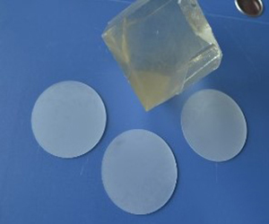
| Material | Sapphire |
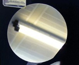
| Wafer Diameter | 76mm, 100mm, 150mm |
| Purity | 99.996% |
| Epi-layer thickness, um | 0.3-2.0 |
 At present, the most common substrate used for the growth of GaN is silicon on a sapphire substrate. The advantage of SOS is that its excellent electrical insulation can effectively prevent radiation caused by scattered current from spreading to nearby components. It also features good chemical stability, no visible light absorption, moderate price, and relatively mature manufacturing technology.
The essence of (SOS) is a heteroepitaxial process, that is, a thin layer of SI (typically less than 0.6 microns) is grown on a sapphire wafer. SOS belongs to the silicon epitaxial technology on an insulator substrate in CMOS technology (SOI) Because of its inherent radiation resistance, SOS is mainly used in aerospace and military applications.
| Parameters range for Silicon on Sapphire (SOS) Epi Wafers | |
| Wafer diameter | 76 mm, 100 mm, 150 mm |
| Orientation | (1012) ± 1o (R-plane) |
| Epi-layer thickness, um | 0.3-2.0 |
| Epi-layer dopant | Phosphorous, Boron |
| n-type | according to spec. |
| p-type | 1,0 – 0,01 |
| Cleaning/packaging |
Class 100 clean room cleaning, vacuum packaging 25 pieces in one cassette packaging or individual packaging. |
Used as the substrate for the growth of III-V compounds such as GaN for LED's.
Used in aerospace and military applications
Our Sapphire Epitaxial Wafer is carefully handled during storage and transportation to preserve the quality of our product in its original condition.